PCB design is the process of creating printed circuit boards that interconnect electronic components to form functional electronic circuits.
1. August 2023
3 minutes reading
Definition of PCB (Design)
PCB stands for "Printed Circuit Board," which is referred to as "trykt kredsløbskort" in Danish. It is a critical component in most electronic devices, providing a structured platform to interconnect and assemble electronic components efficiently and reliably.
In a PCB, a non-conductive material (substrate), usually made of fiberglass or epoxy, is used as a base. On this substrate, a layer of conductive material (often copper) is applied, forming the electrical connections and traces that interconnect the components. PCB design enables electrical connections, creating a circuit that allows the device to perform its specific functions.
The printed circuit board offers several advantages, including compact design, easy mass production, reduced wire clutter, and noise-resistant connections. PCB design is a crucial discipline in electronics, as it facilitates the development of various electronic devices such as computers, mobile phones, TVs, medical equipment, automotive electronics, and many other electronic appliances and systems.
Purpose
PCB design is the process of creating a layout or drawing for a printed circuit board (PCB) that meets the specific requirements of an electronic device or system.
It involves designing the arrangement of components, their interconnections, and the necessary electrical pathways on the PCB to ensure proper functionality and performance.
The process for PCB Design
The PCB design process typically follows these steps:
Requirement Analysis The first step in a PCB design process is to understand the requirements of the electronic device or system for which the PCB is to be designed. This includes factors such as desired functionality, size constraints, power requirements, signal integrity, and environmental conditions.
Schematic Design Schematic design serves as a graphical representation of the circuit, showing the connections and relationships between various electronic components. The functional aspects of the circuit design are considered by representing each component with an appropriate symbol. Connections between components are represented by lines or wires connecting the component symbols. Additionally, a schematic may include other elements such as power and ground symbols, indicating the power supply and reference points in the circuit.
Component Selection The selection of PCB components is based on the schematic. These components must meet the electrical and mechanical requirements of the design. Factors such as availability, cost, performance, and size of the components are considered during this phase. Utilizing a component database can greatly contribute to a more efficient design process and reliable PCB design.
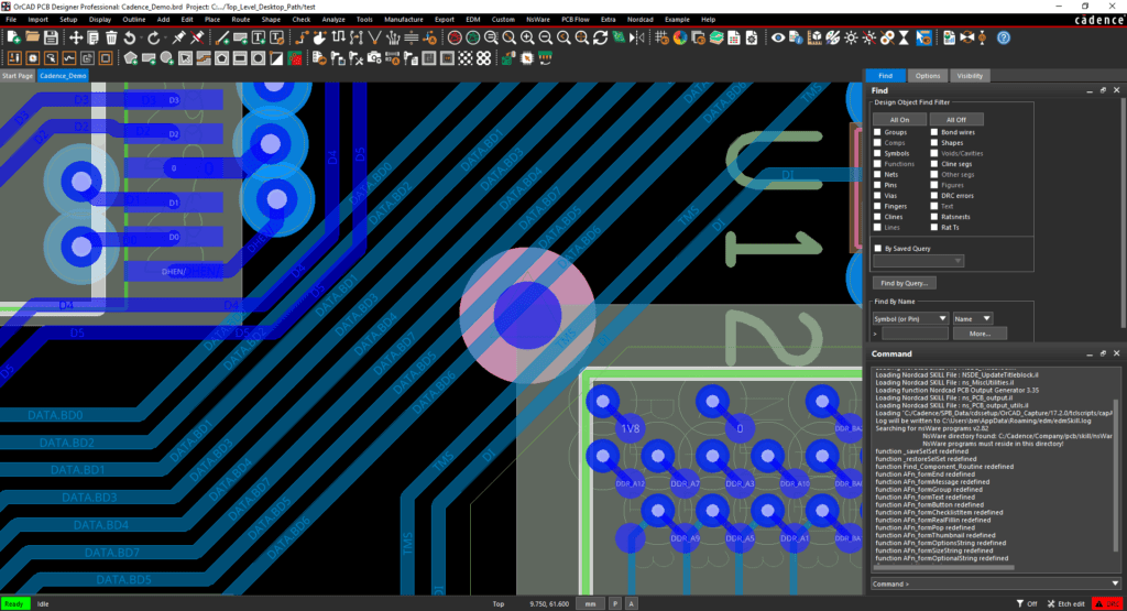
Layout Design The next step involves translating the schematic into a physical PCB layout. Using design software, the components are placed on the circuit board, and their interconnections are routed using copper traces. This phase takes into account factors such as signal integrity, power distribution, thermal management, and electromagnetic compatibility (EMC).
Routing Routing refers to the process of establishing electrical connections between components on the PCB by designing copper traces. To determine the best routing strategy, factors such as signal integrity, noise minimization, and overall layout optimization are considered.
Simulation PCB simulation involves using specialized software tools to simulate and analyze the behavior of a circuit design. Simulation allows engineers to predict and evaluate the electrical characteristics, signal integrity, and performance of the PCB design under different operating conditions. By simulating the circuit, potential issues or errors in the design can be identified and rectified before proceeding to prototype testing.
Design Rule Check (DRC) Once routing for PCB design is completed, a design rule check is performed to ensure that the design complies with specific guidelines, both electronic and production-related. This includes checks for clearances, minimum trace widths, and other design constraints. Understanding these constraints beforehand helps reduce the risk of a failed DRC.
Export of Gerber Files After the DRC is completed, the PCB layout is exported in Gerber file format. Gerber files contain the necessary information for PCB manufacturing, including copper layers, solder mask, and silkscreen layers.
Prototype and Test A PCB prototype is based on the preceding design files. It is assembled with the appropriate components and sent for testing to verify functionality and performance. Any errors found during testing are addressed by iterating the design.
Production Once the design is finalized and validated, the design files are sent to a manufacturer for mass production of the board. The manufacturer follows the specified guidelines to produce the desired quantity of PCBs.
PCB design requires a combination of technical expertise, knowledge of electronic components, and proficiency in using dedicated tools. It is a critical step in electronics development, as a well-designed PCB can significantly impact the overall performance, reliability, and manufacturability of the final product.