


In PCB design, engineers constantly face the challenge of ensuring optimal performance and reliability of their designs.
Two key methods employed in this process are testing and simulation. These techniques play vital roles in validating designs, uncovering potential issues, and optimizing the overall functionality of PCBs.
What is testing?
Testing involves physically evaluating a PCB design to verify its functionality and performance. This process typically involves the following steps:
- producing a physical prototype of the PCB.
- assembling it with components.
- subjecting it to various tests under real-world conditions.
Test setups may include environmental, electrical, and functional testing, among others.
The main advantage of testing is its ability to provide accurate real-time results by directly measuring the physical characteristics of the design.
Additionally, you are also able to uncover issues that may not be apparent through simulation alone.
By physically interacting with the prototype, it allows the engineers to validate the performance of the design in real-world scenarios, accounting for factors such as noise, signal integrity, and thermal effects.
However, testing also comes with its two main limitations.
Time and cost
Testing can be very time-consuming and costly, involving the manufacturing of prototypes, setting up test equipment, and conducting comprehensive testing procedures.
Additionally, some issues may only become apparent during the later stages of the testing process. Which can potentially lead to delays in the development cycle.
We all know that time is money, and multiple delays will hurt your company wallet.
Not only in terms of development but also in terms of materials and other internal resources.
Some advanced testing methods are a good example of this.
Take a method such as reliability testing or in rare cases, destructive testing.
Both may require sacrificing prototypes, which makes it impractical for large-scale manufacturing or costly for limited resources.
Limited coverage
Physical testing has its natural limitations, as it cannot always cover all possible scenarios and edge cases.
This leaves room for potential issues to arise in specific situations that were not tested.
Moreover, your prototypes may not fully represent the final product in terms of materials, manufacturing processes, or component variations.
This potentially leads to discrepancies between the tested prototype and the actual final product.
Maybe testing isn’t feasible or practical for your specific designs, as it may be involving high frequencies, complex interactions, or unsafe environments.
In such cases, the effectiveness would be limited.
Traditional PCB workflow
In traditional PCB workflows, simulation methods aren’t as advanced, precise, and frequent as they are today.
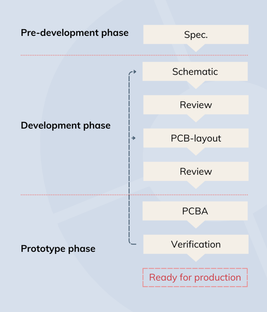
When the specifications of the design are confirmed, engineers would move on to:
- designing the schematic of the PCB,
- followed by a review,
- then designing the PCB layout,
- and lastly, move on to another review before PCBA.
After the PCB assembly, you would begin to test the design to verify that it works as intended.
But if it doesn’t work and you’ve made an error, then the trouble begins.
You’ll have to troubleshoot what caused the error, and that can be very time-consuming, because you may not have any direct indications of the root cause.
Unfortunately, these are some calculated risks that many engineers deal with on a regular basis.
This results in wasted time, money, and delayed manufacturing.
This is exactly why simulation has become an invaluable tool.
What is simulation?
A simulation is a virtual approach for validating your PCB design.
Basically, it involves using specialized software to model the behavior of the PCB and its components based on mathematical algorithms and physical models.
By inputting various parameters and conditions into the software, engineers can simulate the electrical, thermal, and mechanical characteristics of the design.
And additionally, predict its performance without the need for physical prototypes.
There is no doubt that simulation comes with certain advantages.
Diversity and analysis
Simulation allows engineers to quickly iterate and evaluate different design options and enables faster design cycles. Without the need for physical prototypes.
The possibility of exploring different design options and evaluating their impact on performance allows for optimization and fine-tuning of the PCB before committing to the actual manufacturing of the design.
Simulating the PCB under various conditions, such as electrical, thermal, and mechanical stresses, allows you to predict and optimize performance characteristics.
This leads to valuable insights into the behavior of the PCB design, as well as important feedback regarding component status, datasheets, and updates.
Cost reduction
Through simulation, engineers can identify and address potential issues early in the design process.
Early simulations help potential risks and failure modes, enabling proactive measures to be considered, improve reliability, and prevent design flaws before manufacturing.
This can reduce costs that would otherwise be incurred in prototype revisions, and physical testing, and reduce the development costs associated with manufacturing. Such as materials wasted, time, the salary of employees, lost revenue, etc.
Avoiding critical design errors early minimizes the risk of expensive mistakes and poor quality of the finished product overall.
Limitations of simulation
First, let us address the learning curve that comes with implementing simulation software into your toolkit.
It’s not exactly a limitation, but we want to prepare you if your company chooses to implement simulation in the future.
Like with all other beginnings, learning new software takes time.
Time and education you need to invest in to gain invaluable know-how, you can leverage for all eternity.
Nevertheless, simulation can have its limitations if not used in a thoughtful manner, and if you don’t know what you are working with.
It heavily relies on accurate models and assumptions, which can introduce errors if not carefully validated.
The accuracy of simulation results is directly dependent on the quality of the input data and the model’s ability to accurately represent real-world conditions.
Additionally, simulation tools may not account for all physical phenomena, leading to certain limitations in accurately predicting the behavior of complex designs.
Modern PCB workflow
A modern workflow for PCB design is of cause, not surprisingly, based on traditional methods, but with a more strategic and methodical approach to simulation.
Below you’ll see a rough illustration of a modern workflow.
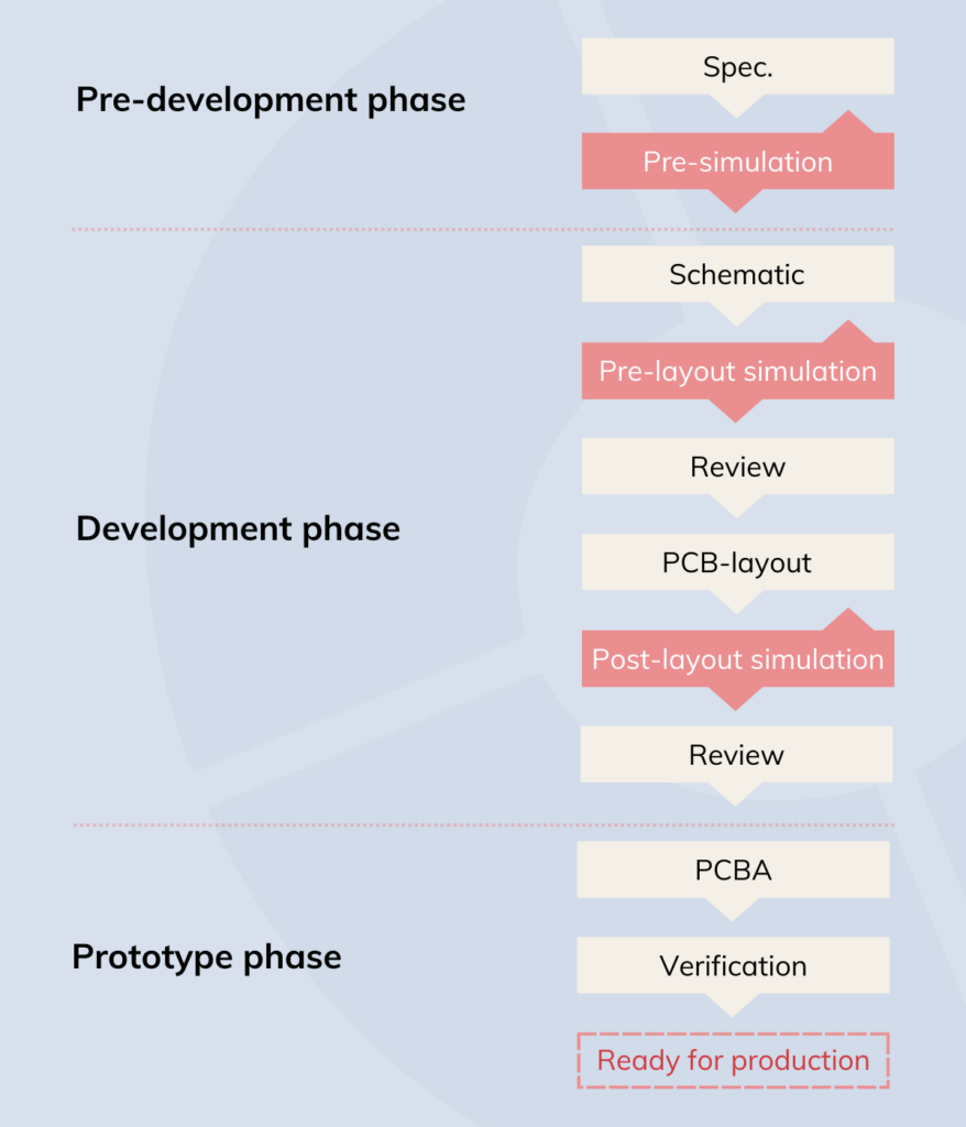
It shows how the simulation works as a gatekeeper preventing errors from progressing to key activities in the workflow.
Every time a key activity like requirement specializations, schematic, or layout, has been completed, you would want to simulate the design for potential errors or issues.
This gives you early indications of things you otherwise would have discovered later (too late) in the validation process.
With simulation, engineers don’t have to live with the constant fear of potential rework.
And managers won’t have to include “rework” as a calculated expense in their budgets.
Stay up-to-date with the latest PCB insights
📺 Webinar: Save time and start using simulation on your circuits
An overview of the benefits of using simulation and how to utilize tools to avoid mistakes.
📺 Webinar: Benefits of nonlinear simulations for your RF design
How to predict performance and optimize the power consumption of your designs.
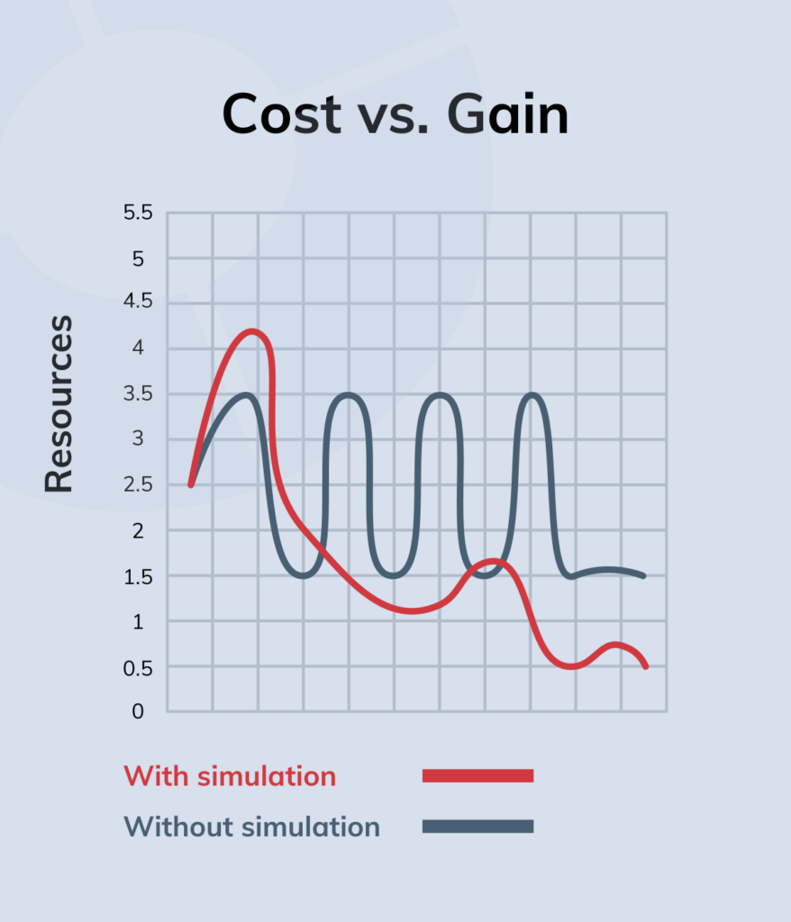
Test vs. Simulation: Which one is better?
First, let’s have a quick recap.
In the illustration below, you’ll see a thought-out example of how an investment in simulation would look like.
As mentioned earlier, a PCB workflow without simulation will have higher costs, because of the potential reworks and waste.
Don’t let the initial steep curve of simulation scare you.
The long-term wins of implementing simulation outweigh the cost of time spent on education and acquiring the tools.
And even better, you only have to make the investment once.
3 tips for implementing both approaches
In conclusion, both testing and simulation are essential tools for achieving PCB design success.
Understand that the implementation of simulation doesn’t mean the exclusion of testing.
In fact, testing is still mandatory.
But simulation will set you up for success in the long run, if used appropriately.
Here are our top three recommendations for using both approaches together.
1. Exploration and optimization
Begin the design process by leveraging simulation tools to explore different design options and evaluate their performance characteristics.
This allows for faster iterations and cost-effective optimization before committing to physical prototypes.
The simulation will help identify potential issues early on and guide the rest of your design decisions and improve overall performance.
2. Validation and targeted testing
Once a design has been simulated and optimized, it is crucial to validate the simulation results by conducting targeted testing on physical prototypes.
This helps to ensure that the simulation accurately represents the real-world behavior of the PCB.
Focus on testing specific aspects or critical areas identified during simulation.
Do this to verify the simulation’s accuracy and identify any discrepancies or unforeseen issues.
3. Reliability assessment
Testing plays a vital role in validating the design’s performance under real-world conditions.
After initial simulations and optimizations, prototype PCBs should undergo comprehensive testing to evaluate their functionality, reliability, and adherence to industry standards.
Factors such as environment, component variations, or complex interactions may not have been uncovered in the simulation, because they haven’t been accounted for in the initial input data.
The results from testing can then be used to refine the simulation models and improve future designs.