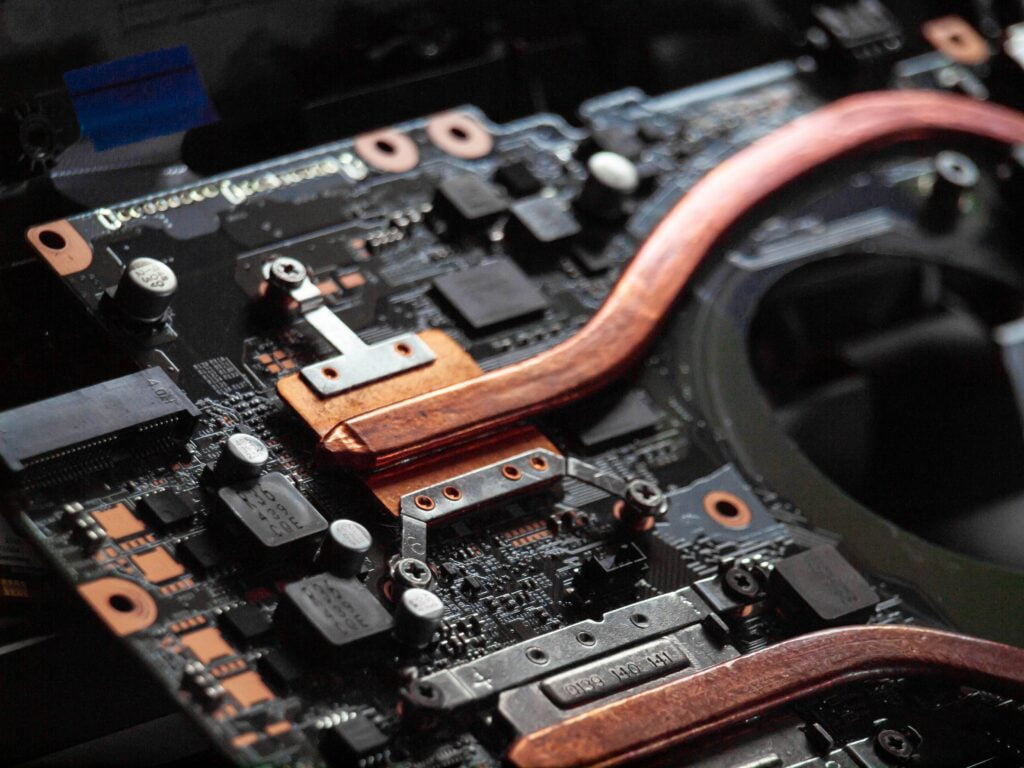
A printed circuit board (PCB) is a fundamental component in electronics manufacturing that functions as a platform to assemble and connect various electronic components to create functional devices. It is typically a flat, rigid, or flexible board made of insulating material such as fiberglass, with conductive traces etched on the surface. These traces provide electrical connections that link components such as resistors, capacitors, integrated circuits, and connectors, enabling the flow of signals and currents.
Definition
A PCB is an essential building block in modern electronics.
It typically consists of a non-conductive substrate material, often made of fiberglass-reinforced epoxy, known as the printed circuit board. This base material provides mechanical support and stability to the components mounted on it.
On the surface of a printed circuit board, there are conductive pathways called traces or copper traces, which form the electrical connections between the components. These copper traces are created by etching or printing a thin layer of copper on its surface.
Electronic components such as integrated circuits (ICs):
Resistors
Capacitors
Transistors
Connectors
These are mounted on the PCB using various soldering techniques.
The components are positioned and secured at designated locations on the board, and their pins or terminals are soldered to the copper traces.
This soldering process establishes electrical connections between the components and the PCB, forming a complete circuit.
All components are represented by a footprint, which shows the electrical pins, component size, a mechanical 3D model, and documentation details.
Overview of PCB building blocks
Substrate: The substrate, also known as the board base material, is the foundation on which the board is built. It provides mechanical support and electrical isolation for the circuit.
Common substrate materials include fiberglass-reinforced epoxy (FR-4), polyimide (PI), and Rogers materials.
Copper Layers: Copper layers are thin layers of copper laminated onto the substrate. These layers act as conductive pathways for electrical signals and power distribution.
The PCB can have constructions with single-layer (one copper layer), double-sided (two copper layers), or multilayer (three or more copper layers).
Pads: Pads are small areas of exposed copper on the PCB surface. They act as contact points for soldering electronic components onto the board.
Pads provide electrical connections between the components and copper traces.
Vias: Vias are small plated holes in the PCB that establish connections between different layers. They allow traces to pass from one layer to another, enabling complex circuits and efficient space utilization.
Vias can be through-hole vias (connecting all layers) or blind/buried vias (connections between specific layers).
Solder mask: The solder mask is a protective layer applied over copper traces and pads. It is usually green but can also be in other colors. The solder mask prevents solder bridges and unintended connections during soldering, while also protecting copper traces from environmental factors and corrosion.
Silkscreen: The silkscreen layer is a non-conductive layer containing markings, labels, component outlines, reference designators, and other text or symbols. It provides information for assembly, identification, and reference purposes, aiding in component placement and orientation.
Components: Electronic components are the functional elements mounted on the board to form the electronic circuit. This includes integrated circuits (ICs), resistors, capacitors, inductors, diodes, transistors, connectors, and various other active and passive components.
Mounting Holes: Mounting holes are pre-drilled holes on the PCB used to attach the board to a chassis or a larger system. They provide mechanical stability and proper alignment of the board during installation.
Power- and Ground Planes: Power and ground planes are dedicated copper layers in multilayer PCBs that carry power and ground signals, respectively. They provide low-impedance paths for power distribution, reduce noise, and aid in signal integrity.
These building blocks work together to create a functional PCB.
Engineers strategically place and route the traces, position the components, and optimize layer structure to meet electrical, mechanical, and manufacturing requirements.
The interplay of these elements forms the circuit, enabling the desired functionality of the electronic device or system.
Implementation
he process of creating a PCB involves several steps, including design, layout, fabrication, and assembly:
Design: Engineers use specialized software to design the layout of components and traces. This involves factors such as signal paths, component placement, and thermal management.
Layout: The designed layout is transformed into a physical representation using computer-aided design (CAD) tools. This includes defining positions and sizes of components, traces, vias, and pads.
Fabrication: The PCB design is transferred to a physical board through processes like etching. A copper-clad board is etched to create the desired conductive traces and patterns.
Assembly: Electronic components are soldered onto the PCB using automated assembly equipment. Methods like surface mount technology (SMT) or through-hole technology (THT) can be used.
Benefits
PCBs offer a variety of advantages that contribute to the efficiency and reliability of electronic systems:
Compact Integration: PCBs allow complex electronic circuits to be compactly integrated, reducing space requirements and enabling device miniaturization.
Improved Signal Integrity: Well-designed PCBs minimize signal distortions, crosstalk, and electromagnetic interference, leading to higher signal integrity and better system performance.
Easy Manufacturing: Standardized manufacturing processes make PCB assembly efficient and cost-effective, enabling mass production of electronic devices.
Design Flexibility: PCBs can be designed for specific applications, allowing customization of component placement, routing, and performance characteristics.
Reduced Interconnect Length: PCB design optimizes the distance between components, reducing signal travel times and minimizing delays.
Reliability and Reproducibility: PCBs provide consistent electrical connections, reducing the risk of connection errors and ensuring reproducibility in manufacturing.
In summary, PCBs are essential components in modern electronics, offering an organized and efficient method of connecting electronic elements. Through precise design, fabrication, and assembly processes, PCBs contribute to the reliability, performance, and miniaturization of a wide range of electronic devices and systems.