Signal integrity (SI) is the discipline of ensuring that electrical signals preserve their quality, timing, and shape as they travel through a PCB or electronic system. Strong SI prevents reflections, crosstalk, and noise-related failures, which are critical for reliable high-speed designs. Engineers, hardware designers, and system architects rely on SI analysis to build robust electronics that meet performance and regulatory standards.
Why signal integrity matters in modern electronics
As data rates and frequencies increase, SI becomes a critical factor in high-speed PCB and system design. Proper SI ensures:
Error-free communication between components and subsystems
Stable operation in noise-sensitive, high-frequency environments
Minimization of EMI/EMC issues and compliance with regulatory standards
Durable, reliable designs in critical applications
Higher production yield and fewer field failures
Industries such as telecom, aerospace, automotive, and industrial automation rely on strong SI to deliver competitive, dependable products.
Signal integrity vs. traditional electrical design
While traditional electrical design focuses on connectivity, power, and components, signal integrity examines how signals actually behave in real-world high-speed circuits.
Aspect
Signal Integrity
Traditional Electrical Design
Focus
Signal shape, timing, impedance, reflections, noise
Net connections, component selection, power distribution
With rising frequency and miniaturization demands, SI is an unavoidable part of professional PCB design.
Integrating Signal Integrity into Hardware Development
Applying signal integrity analysis early in the hardware design process gives teams the ability to anticipate and resolve high-speed signal issues before they become costly problems. By embedding SI workflows from the start, engineers can ensure more predictable performance, reduce design iterations, and build more robust systems.
Key benefits of integrating SI early:
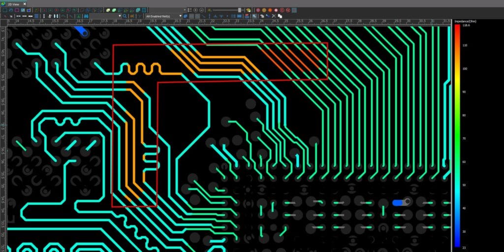
Prevent signal distortion and data corruption before prototyping: Early simulation and analysis allow engineers to detect reflections, crosstalk, or impedance mismatches in critical traces, ensuring signals maintain their shape and timing throughout the PCB. This reduces the risk of failures in prototype boards and avoids costly rework.
Reduce EMI/EMC failures and costly redesigns: Identifying potential sources of electromagnetic interference early helps teams design boards that comply with regulatory standards. By simulating high-frequency behavior and verifying impedance matching, designers can prevent time-consuming EMC issues during testing or certification.
Ensure data integrity in high-speed interfaces such as PCIe Gen4–6, USB-C, DDR, and Ethernet: For modern electronics, interfaces operate at multi-gigabit speeds where even minor signal degradation can cause data errors. Pre-layout SI simulations and post-layout verification help maintain signal fidelity, timing, and synchronization across all critical paths.
Optimize layout and routing through pre- and post-layout simulations: Integrating SI into the design workflow enables engineers to make informed layout decisions, such as trace length adjustments, differential pair routing, via placement, and layer stack optimization. This leads to more predictable signal behavior and fewer revisions.
Shorten time-to-market with fewer iterations and higher-quality output: By catching signal integrity issues early, teams can reduce the number of prototype cycles, minimize redesigns, and achieve first-pass success in high-speed PCB validation. This not only accelerates project timelines but also improves overall design reliability and yield.
Who Benefits from Signal Integrity?
Signal integrity is critical for anyone working with high-speed or complex electronic systems. Mistakes are costly, and proactive SI analysis pays off technically and financially.
Typical users include:
Hardware designers and PCB engineers
System architects handling high-speed interfaces
R&D teams in regulated or performance-critical industries
QA managers and test engineers
Companies focused on EMC, CE, and regulatory compliance
For products requiring international certification or operating in high-EMI environments, SI is essential—not optional.
Best practices to get started with Signal Integrity
A successful approach to signal integrity begins with understanding your current PCB design workflows. Map how signals travel through traces, vias, and components, and identify where distortions, reflections, or EMI might occur—these are your opportunities for improvement.
Practical steps to get started:
Start small with a pilot project on a single high-speed interface, such as PCIe, DDR, or USB-C.
Define ownership and responsibility for SI verification and analysis in your team.
Involve all relevant stakeholders early—especially hardware designers, layout engineers, and system architects.
Choose SI tools and workflows that integrate with your existing PCB design environment, supporting pre- and post-layout simulation, impedance verification, and compliance checks.
Nordcad provides advanced SI tools and workflows that integrate directly with OrCAD and Allegro environments. This allows engineers to simulate, verify, and optimize signal integrity without leaving their familiar PCB design tools, ensuring robust, high-speed designs from the first iteration.
Additional ressources
Webinars
Watch our webinars on SI and signal integrity analysis.