










There is a question we hear more and more often: Is AI in PCB design actually relevant to me?
It is a fair question. The stories you read usually feature large, global companies with thousands of components on a board and impressive percentages in the headline. It is easy to conclude that this is for them – not for a team of five, or one, for that matter.
But that conclusion does not quite hold. The AI technology behind the big results is not locked away in an enterprise platform. It runs in the same tool that many already use.
So the question is not whether AI is relevant to you. It is where in your process it makes a difference – and what it looks like when you actually sit down with it.
AI or just automation?
Before looking at the tools, it is worth keeping two concepts apart. They are often (unknowingly) mixed up, and they solve different kinds of tasks.
Automation is what you already know: tasks with one right answer and a fixed process. A DRC check. A BOM generated from a netlist. Batch renaming of components. The rules are known in advance, and the tool carries them out faster and more consistently than a person. But it does not make decisions along the way.
AI makes sense when a task has many possible solutions, and the best one depends on a trade-off. How are hundreds of components best placed in relation to each other? How do you balance signal integrity and board space at the same time? There is no single right answer here. There is a solution space that AI can explore faster than an engineer can by hand.
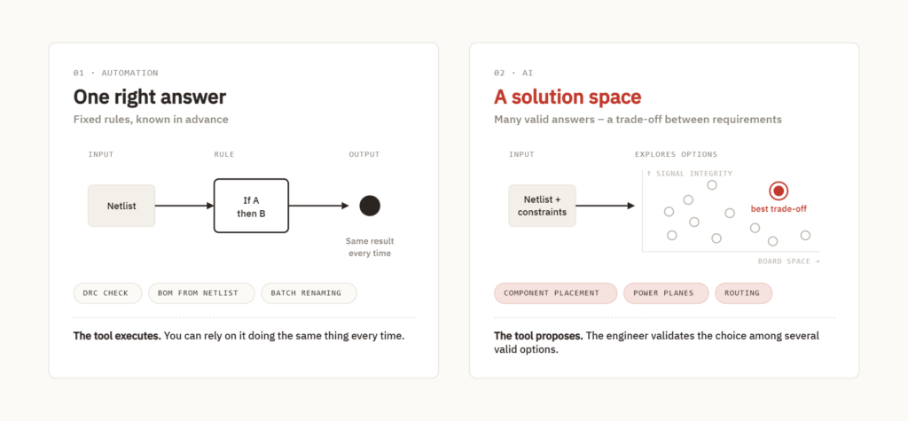
The difference matters in practice. An automated task can be trusted to do the same thing every time. A result from AI should always be reviewed – not because it is unreliable, but because it is one choice among several valid options. That choice is one you need to be able to stand behind.
Where AI in PCB design belongs in your workflow today
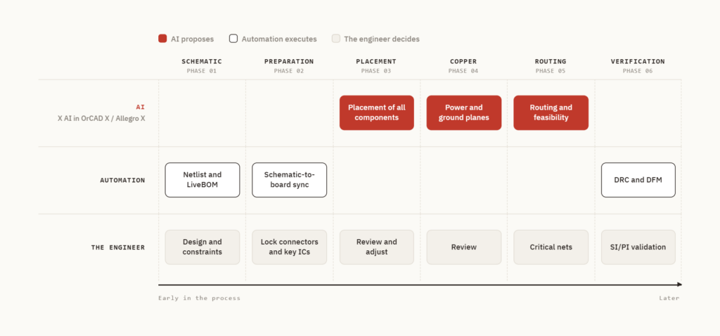
Cadence's technology for AI in PCB design is called Allegro X AI, and in the tool you simply find it as X AI. It targets the layout phase – where the heavy, time-consuming part of the work lies. In concrete terms, it does three things:
- Placement – places components based on the netlist, your constraints, mechanical restrictions and assembly rules.
- Copper – generates power and ground planes based on the voltages and layers you have defined.
- Routing – routes the board or is used for quick feasibility studies: Can this actually be routed on four layers?
What many people overlook is that X AI is not limited to Allegro X, Cadence's enterprise platform. It also runs directly in OrCAD X from version 25.1. You work in the same environment you are used to, and the result lands in your own board.
A few practical points about AI in PCB design are worth knowing up front. The computation currently runs in Cadence's secure cloud environment on AWS, and an on-premises option is being rolled out for companies that need to keep data local. X AI supports boards with up to 5,000 components, but not yet flex or rigid-flex.
What it looks like in practice
When you open X AI for the first time, it is less exotic than you might expect. It takes place in a panel in the PCB tool you already know, and it follows four steps.
1. Open Allegro X or OrCAD X and upload the board. Under Tools › X AI, you log in, create a workspace and upload the board you have open.
2. Describe the design. This is where the work lies. You define component classes – which parts are ICs and which are connectors – the spacing between classes, and which layers your power and ground nets should use. If you have decoupling capacitors that need to sit at specific pins, you can specify this with component associations. Connectors, switches and the one or two most important ICs are locked in advance.
3. Run. Choose whether X AI should place components, generate copper or both, and click Run X AI. You can run several variants in parallel and compare strategies. Some runs take minutes, others hours, depending on the complexity of the board.
4. Review. The result is downloaded into your board, and then it is your turn. If you are not satisfied, moving components around by hand is rarely a good idea. Instead, adjust the constraints that led to the result and run it again. That way your design intent gets written down, and the next run gets closer.
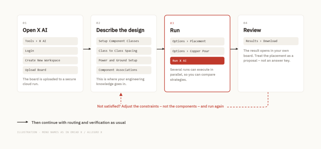
After that, you continue with routing and verification as usual.
What it means on a smaller board
In a test on a board with 80 components and four layers, the two approaches were compared directly. Configuring the design rules took 10 minutes – that has to be done whether you place by hand or with AI. After that, the AI-specific setup took 5 minutes, the run itself 2 minutes and the review 8 minutes. In total, 25 minutes compared to around 70 minutes for manual placement.
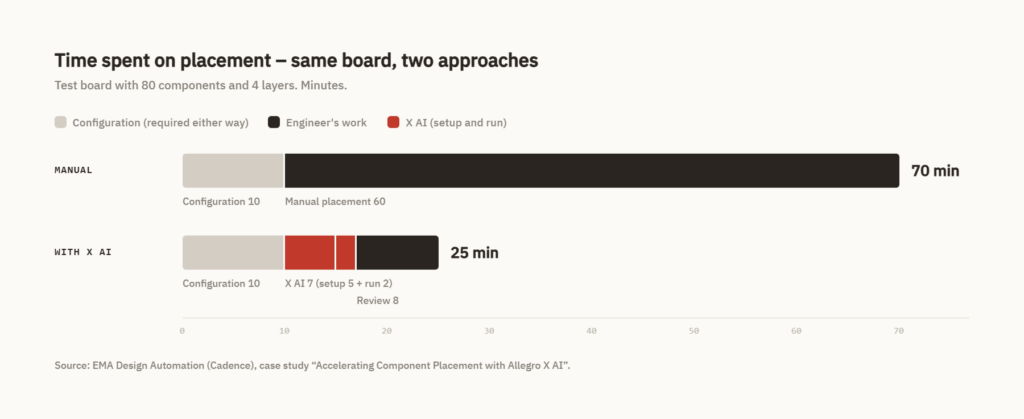
The result was not perfect, and that is worth mentioning. During the review, some capacitors and resistors had ended up on the bottom layer, and the components were packed so tightly that routing could become harder. The engineers solved this by adjusting the constraints rather than moving components by hand.
It gives a realistic picture of the gain from AI in PCB design on a smaller board. It is not measured in days, but in hours that can be spent on design decisions instead of routine placement. And the gain grows with the number of components.
When does it make sense – and when does it not?
AI in PCB design is not the answer to everything, and there is no reason to pretend otherwise. A few rules of thumb:
It typically makes sense when …
You are starting a new board with many passive components. This is where the biggest time saving lies, because a large part of the placement is routine.
You need an early feasibility study. Will everything fit on the board? How many layers will it take? An AI run gives a realistic estimate before you have spent days on it.
A design changes between two revisions. AI can quickly provide a new starting point when the assumptions shift.
It typically makes less sense when …
The board is very small. With a handful of components, an experienced designer will often place them faster than it takes to set up X AI.
Placement is dictated by physics. RF sections and sensitive analogue circuits, where every millimetre is a deliberate decision, you place yourself – and lock before AI takes care of the rest.
It is flex or rigid-flex. This is not supported today.
And what about the schematic?
There is no equivalent "AI button" in schematic capture itself today. But what happens at schematic level is just as important for how well the AI performs later in the process.
A clean netlist, correctly defined constraints and up-to-date component data via LiveBOM are the foundation X AI works from. If you assign voltages to your DC nets already in the schematic, part of step 2 above is already done. That is automation, not AI – and there is nothing wrong with that. The better the foundation, the better the result. It is the same logic as in simulation: decisions made early determine how much value you can get later.
The direction: from placement to the whole system
Developments over recent months point beyond PCB layout itself. The same type of technology is starting to accelerate multiphysics simulation across thermal, mechanical and signal/power integrity – and to help coordinate decisions across engineering disciplines, so that a system-level design reaches a finished result faster.
This was also something we noticed clearly when we recently held seminars on the topic in Sweden: the interest is there, the questions are concrete, and it is increasingly not just about one board, but about how it works together with the rest of the system.
What it means, regardless of team size
Danfoss is a good example of what happens when you scale the technology up to a full Allegro X setup: 85% faster component placement on a project with thousands of components.
But the same technology for AI in PCB design runs in OrCAD X – whether you are five engineers or five hundred. The difference is the scale of the task, not access to the technology.
If you want to try it out, a board you already know well is the best place to start. That way you can compare the AI's proposal with your own placement and see where it gets it right, and where your experience still makes the difference.
If you are curious about where AI in PCB design can make a concrete difference in your own workflow, we can look at your setup, including how X AI fits with your licence, and point out where it makes sense to start.