









There's a consistent pattern in how engineering teams structure their PCB simulation workflow — and it tends to produce the same outcome, over and over again.
The board comes back from fabrication. Bring-up reveals something unexpected — a supply rail that droops under load, an interface that fails at maximum data rate, or a device that resets under specific operating conditions. Engineers spend days narrowing it down. Simulation eventually confirms the root cause. The fix is straightforward. The respin takes three weeks.
This is the standard sequence. It's accepted as normal. It reflects a PCB simulation workflow built around verification rather than prevention — and it doesn't have to be. The same simulation that confirms a respin would also have prevented it, if it had been run three weeks earlier.
The cost of finding problems late
A board respin has direct costs: fabrication, assembly, engineering time. It also has indirect costs that are harder to quantify — delayed launches, resources pulled from other projects, and the accumulated strain of debugging under schedule pressure.
The problems that cause respins are almost always structural. Impedance mismatches, PDN resonances, IR drop hotspots, return path discontinuities — these are systematic issues that follow from design decisions made during schematic capture and layout. They're not random failures. They're predictable consequences of specific choices. Most of them can be identified before routing begins — but only if the analysis is built into the process at the right point.
The reason they're found late isn't that they're hard to detect. It's that simulation is typically treated as a verification step at the end of the design process — something you do to confirm that a finished layout is correct. By that point, fixing a structural problem often means rerouting significant parts of the board.
That's a PCB simulation workflow problem, not a tooling problem. The tools to catch these issues earlier exist and are widely available. The question is when in the process they're used.
Restructuring the PCB simulation workflow
Moving signal and power integrity analysis earlier doesn't mean running full simulations before any layout exists. It means making simulation an input to design decisions, not just an evaluation of their outcome. The goal is to catch structural issues while there's still time to address them without a respin.
In practice, restructuring the PCB simulation workflow looks like several concrete changes to the sequence of work.
Impedance and stackup defined before routing. Target impedance for critical nets, calculated against the actual board stackup, should be established before a trace is placed. This takes an hour. It determines routing constraints that, if applied consistently, prevent impedance mismatch failures entirely.
PDN design and capacitor selection completed during schematic. PDN impedance analysis can be run with a schematic-level model — before layout geometry exists. This identifies resonance risks and allows capacitor values and types to be optimised before placement. Moving this analysis forward by even one design phase typically eliminates a full category of power integrity failure.
IR drop modelled before copper is poured. A current density model built from the schematic and initial component placement identifies high-resistance paths. Correcting trace widths before routing is finalised is a routing decision. Correcting them after fabrication is a respin.
Return path continuity assessed during component placement. Plane splits, via transitions, and layer assignments that affect return current flow can be evaluated and corrected during placement — before routing begins. At the routing stage, fixing a reference plane problem may mean rerouting multiple layers.
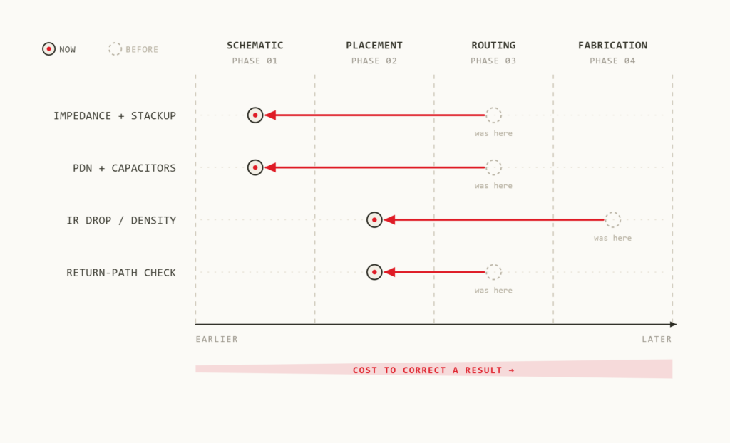
None of these steps require an entirely new PCB simulation workflow. They require the same workflow, reordered. Each move shifts the same analysis to an earlier point in the process. The simulation doesn't change. The cost of acting on the result does.
What this requires
Running simulation earlier requires tools that support pre-layout or concurrent analysis, not just post-layout verification. Cadence Sigrity and the signal integrity features in OrCAD X are designed for exactly this — they allow PDN analysis, impedance modelling, and return path assessment at the stages where it's cheapest to act on the results.
It also requires that simulation be part of the default design workflow, not something that happens when a problem is suspected. For many teams, the barrier isn't skill or tooling. It's habit.
Beyond tooling, the shift requires alignment between the layout engineer and the SI analyst at stages where they don't typically interact. In many teams, signal integrity review happens after layout is complete — because that's when the layout engineer considers the work done and passes it on. Moving that review forward means building explicit checkpoints into the workflow, not relying on a late-stage handoff.
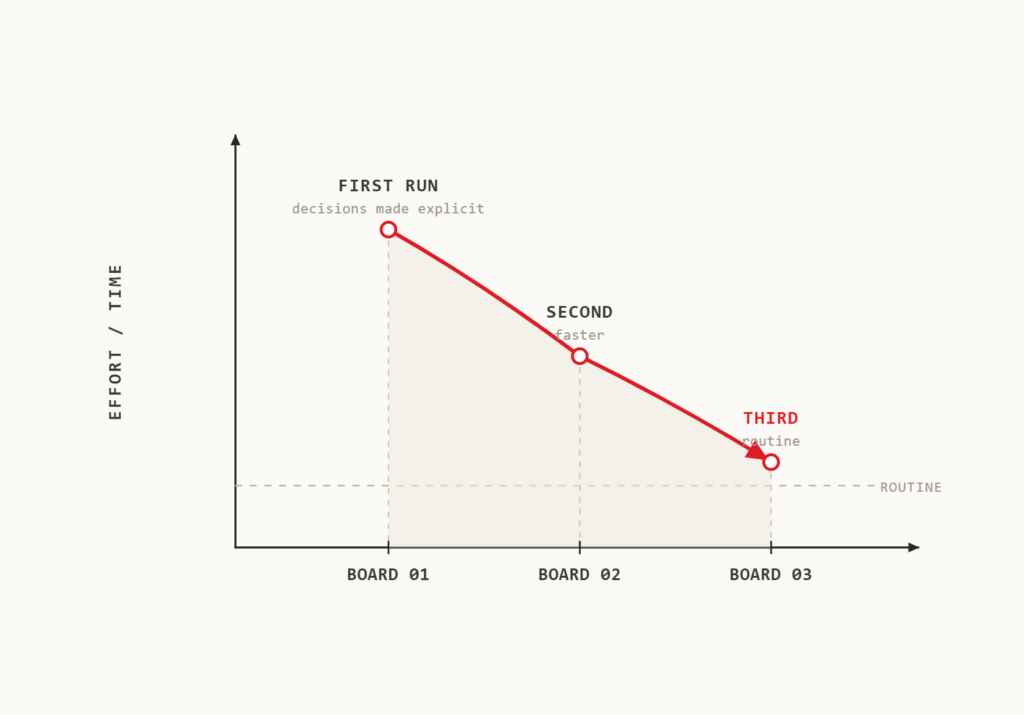
One pattern we see regularly when teams restructure their process: the first pre-layout PDN analysis takes longer than expected, because the team has to make explicit decisions they previously made by intuition. The second run is faster. By the third board, the earlier checks have become routine.
The practical case
The ten most common signal and power integrity issues that cause PCB design failures — impedance mismatch, crosstalk, PDN resonance, IR drop, ground bounce, return path discontinuities, via stubs, inadequate decoupling, timing skew, and EMI leakage — are all catchable before fabrication. Most of them are catchable before routing is complete.
For teams that have restructured their process, the impact shows up in two places: fewer findings at final verification, and shorter debugging cycles when problems do arise. When a failure is caught during schematic review, there's typically one engineer, one constraint, and one decision. When it surfaces during board bring-up, there's a debug session, a root cause investigation, a fix, and a respin.
That's not an argument for a more complicated design process. It's an argument for putting the right checks at the right point in the existing one.
The PCB simulation workflow is the same whether you run it during schematic review or during board bring-up. The cost of acting on the result is not.
If your team works with Cadence Sigrity, OrCAD X, or similar SI/PI tools and wants to build simulation into the design flow from the start, Nordcad's specialists can review your current process and identify where analysis can be moved earlier. We work with engineering teams across the Nordics on exactly this.